- 您现在的位置:买卖IC网 > Sheet目录2002 > LT8500IUHH#TRPBF (Linear Technology)IC PWM GENERATOR 56-QFN
LT8500
4
8500f
Note 1: Stresses beyond those listed under Absolute Maximum Ratings
may cause permanent damage to the device. Exposure to any Absolute
Maximum Rating condition for extended periods may affect device
reliability and lifetime.
Note 2: The LT8500E is guaranteed to meet performance specifications
from 0°C to 125°C junction temperature. Specifications over the –40°C
to 125°C operating junction temperature range are assured by design,
characterization and correlation with statistical process controls. The
LT8500I is guaranteed over the full –40°C to 125°C operating junction
temperature range.
Note 3: Propagation delays, setup/hold times and hi times are measured
from 50% to 50%.
Note 4: This parameter is correlated to lab measurements and is not
subject to production testing.
TiMing characTerisTics The
l
denotes the specifications which apply over the full operating temperature
range, otherwise specifications are at TA = 25°C. VCC = 3.3V, and all inputs are rail-to-rail unless otherwise noted.
SYMBOL
PARAMETER
CONDITIONS
MIN
TYP
MAX
UNIT
tPD-PWM
PWMCK-PWM[48:1] Propagation Delay
(Note 3)
PWMCK
↑ – PWM ↑↓ (Figure 5)
l
32
50
ns
tR-SDO
SDO, SCKO Rise Time (Note 4)
CLOAD = 25pF, 30% to 70%
2
ns
tF-SDO
SDO, SCKO Fall Time (Note 4)
CLOAD = 25pF, 70% to 30%
2
ns
tR-PWM
PWM[48:1] Rise Time (Note 4)
CLOAD = 25pF, 30% to 70%
12
ns
tF-PWM
PWM[48:1] Fall Time (Note 4)
CLOAD = 25pF, 70% to 30%
12
ns
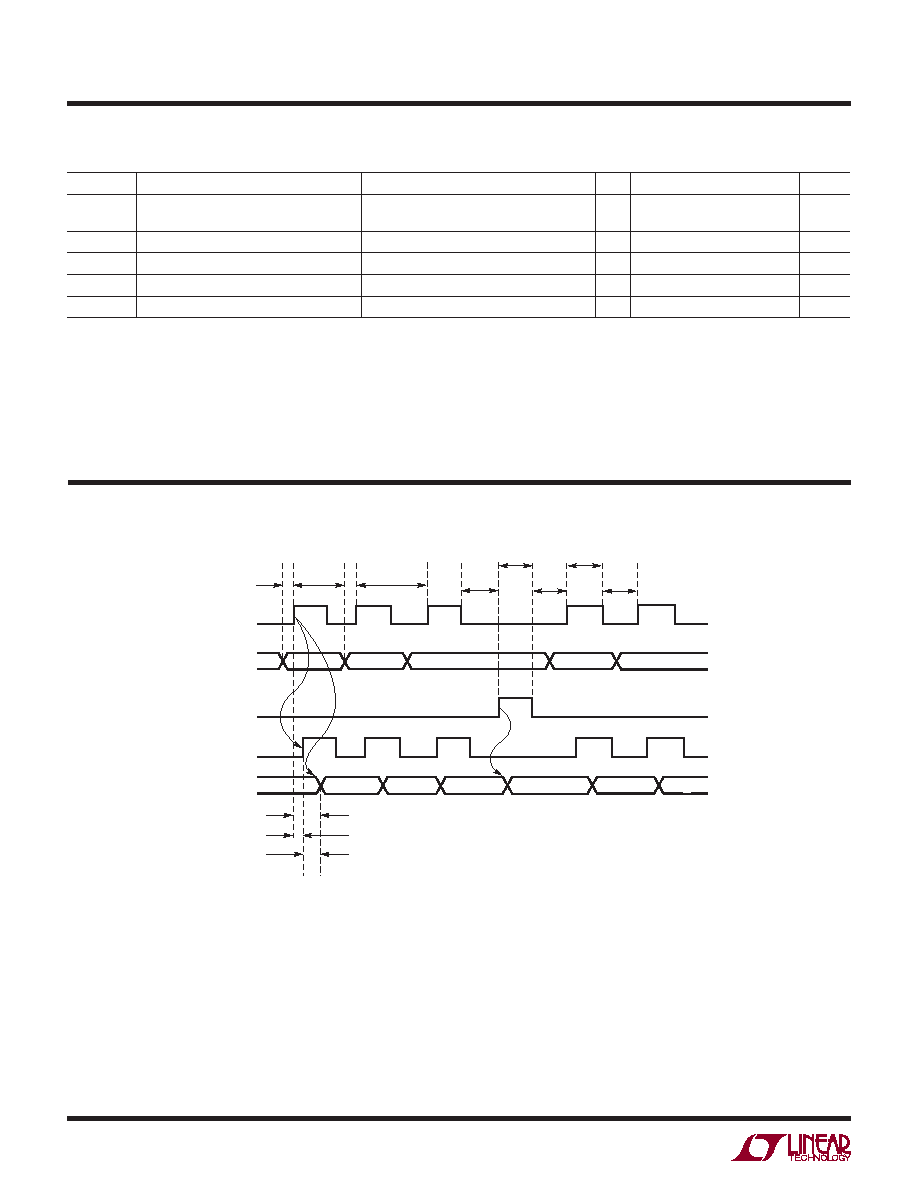
TiMing DiagraM
SCKI
8500 TD01
SDI
LDIBLANK
SDO
SCKO
tSU-SDI
tHD-SDI
tSU-LDI
tWH-LDI
tHD-LDI
1/fSCKI
tWH-SCKI
tWL-SCKI
tPD-SDO
tHD-SDO
tPD-SCK
发布紧急采购,3分钟左右您将得到回复。
相关PDF资料
LTC1096IN8#PBF
IC A/D CONV 8BIT SRL IN/OUT 8DIP
LTC1099ACN#PBF
IC A/D CONV 8BIT HI-SPEED 20-DIP
LTC1197IMS8#PBF
IC ADC 10BIT 500KHZ SHTDWN 8MSOP
LTC1198-1BCS8#PBF
IC ADC 8BIT 750KHZ SAMPL 8-SOIC
LTC1257IS8#TRPBF
IC D/A CONV 12BIT VOLT OUT 8SOIC
LTC1276ACN#PBF
IC A/D CONV 12BIT SAMPLING 24DIP
LTC1278-4IN#PBF
IC A/DCONV SAMPLNG W/SHTDN 24DIP
LTC1279CG#TRPBF
IC A/DCONV SAMPLNG W/SHTDN24SSOP
相关代理商/技术参数
LT-8501M
制造商:Mencom 功能描述:
LT8582EDKD#PBF
功能描述:IC REG MULTI CONFIG ADJ 3A 24DFN RoHS:是 类别:集成电路 (IC) >> PMIC - 稳压器 - DC DC 开关稳压器 系列:- 标准包装:250 系列:- 类型:降压(降压) 输出类型:固定 输出数:1 输出电压:1.2V 输入电压:2.05 V ~ 6 V PWM 型:电压模式 频率 - 开关:2MHz 电流 - 输出:500mA 同步整流器:是 工作温度:-40°C ~ 85°C 安装类型:表面贴装 封装/外壳:6-UFDFN 包装:带卷 (TR) 供应商设备封装:6-SON(1.45x1) 产品目录页面:1032 (CN2011-ZH PDF) 其它名称:296-25628-2
LT8582EDKD#PBF
制造商:Linear Technology 功能描述:DC/DC CONVRTER BOOST INVERTING SEPIC
LT8582EDKD#TRPBF
功能描述:IC REG MULTI CONFIG ADJ 3A 24DFN RoHS:是 类别:集成电路 (IC) >> PMIC - 稳压器 - DC DC 开关稳压器 系列:- 设计资源:Design Support Tool 标准包装:1 系列:- 类型:升压(升压) 输出类型:固定 输出数:1 输出电压:3V 输入电压:0.75 V ~ 2 V PWM 型:- 频率 - 开关:- 电流 - 输出:100mA 同步整流器:是 工作温度:-40°C ~ 85°C 安装类型:表面贴装 封装/外壳:SOT-23-5 细型,TSOT-23-5 包装:剪切带 (CT) 供应商设备封装:TSOT-23-5 其它名称:AS1323-BTTT-30CT
LT8582IDKD#PBF
功能描述:IC REG MULTI CONFIG ADJ 3A 24DFN RoHS:是 类别:集成电路 (IC) >> PMIC - 稳压器 - DC DC 开关稳压器 系列:- 标准包装:250 系列:- 类型:降压(降压) 输出类型:固定 输出数:1 输出电压:1.2V 输入电压:2.05 V ~ 6 V PWM 型:电压模式 频率 - 开关:2MHz 电流 - 输出:500mA 同步整流器:是 工作温度:-40°C ~ 85°C 安装类型:表面贴装 封装/外壳:6-UFDFN 包装:带卷 (TR) 供应商设备封装:6-SON(1.45x1) 产品目录页面:1032 (CN2011-ZH PDF) 其它名称:296-25628-2
LT8582IDKD#PBF
制造商:Linear Technology 功能描述:DC/DC CONVRTER BOOST INVERTING SEPIC
LT8582IDKD#TRPBF
功能描述:IC REG MULTI CONFIG ADJ 3A 24DFN RoHS:是 类别:集成电路 (IC) >> PMIC - 稳压器 - DC DC 开关稳压器 系列:- 设计资源:Design Support Tool 标准包装:1 系列:- 类型:升压(升压) 输出类型:固定 输出数:1 输出电压:3V 输入电压:0.75 V ~ 2 V PWM 型:- 频率 - 开关:- 电流 - 输出:100mA 同步整流器:是 工作温度:-40°C ~ 85°C 安装类型:表面贴装 封装/外壳:SOT-23-5 细型,TSOT-23-5 包装:剪切带 (CT) 供应商设备封装:TSOT-23-5 其它名称:AS1323-BTTT-30CT
LT8584IFE#PBF
制造商:Linear Technology 功能描述:IC BATT CELL BALANCE 16TSSOP 制造商:Linear Technology 功能描述:BATTERY BALANCER, 2.5V-5.3V, TSSOP-16, Supply Voltage Min:2.5V, Supply Voltage M